 NB INSTRUMENT
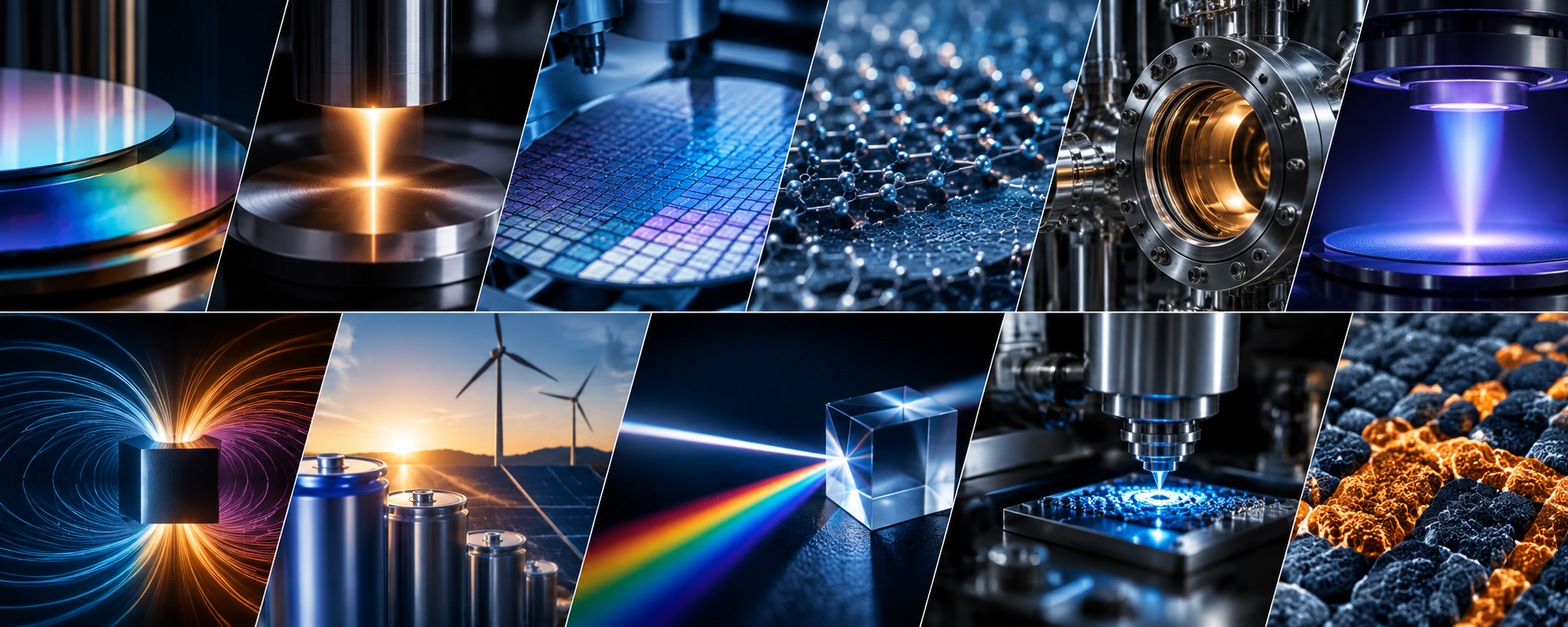
Technology Built Around Your Research
From thin film deposition and surface engineering to semiconductor processing, advanced materials and magnetic research, connect your research objective with the right technology, process and instrumentation.
Where the technology meets the research.
Each area connects to the technology environments and systems most relevant to it.
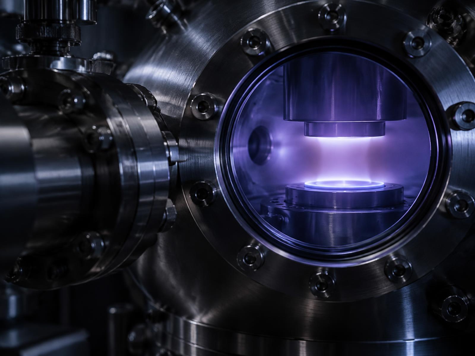
Thin Film Deposition
Engineer controlled films for optical, electronic and protective applications.
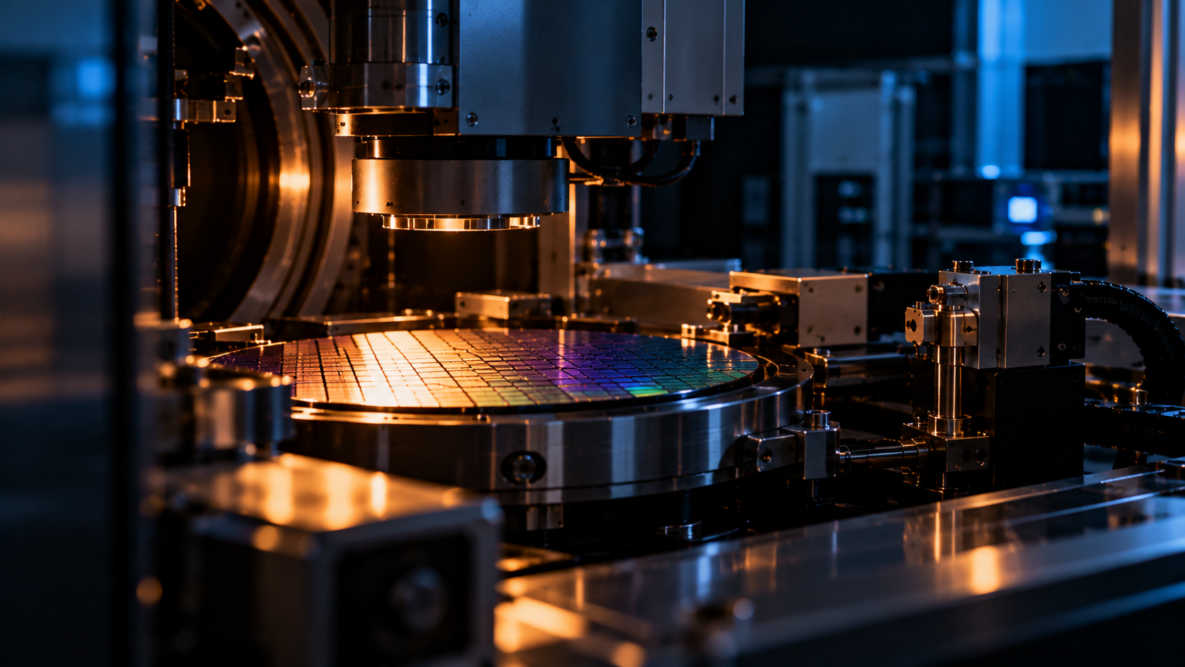
Semiconductor R&D
Support wafer-scale process development and microfabrication research.
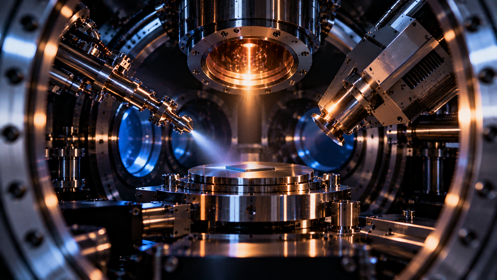
Vacuum & Surface Science
Create stable environments for surface preparation and analysis.
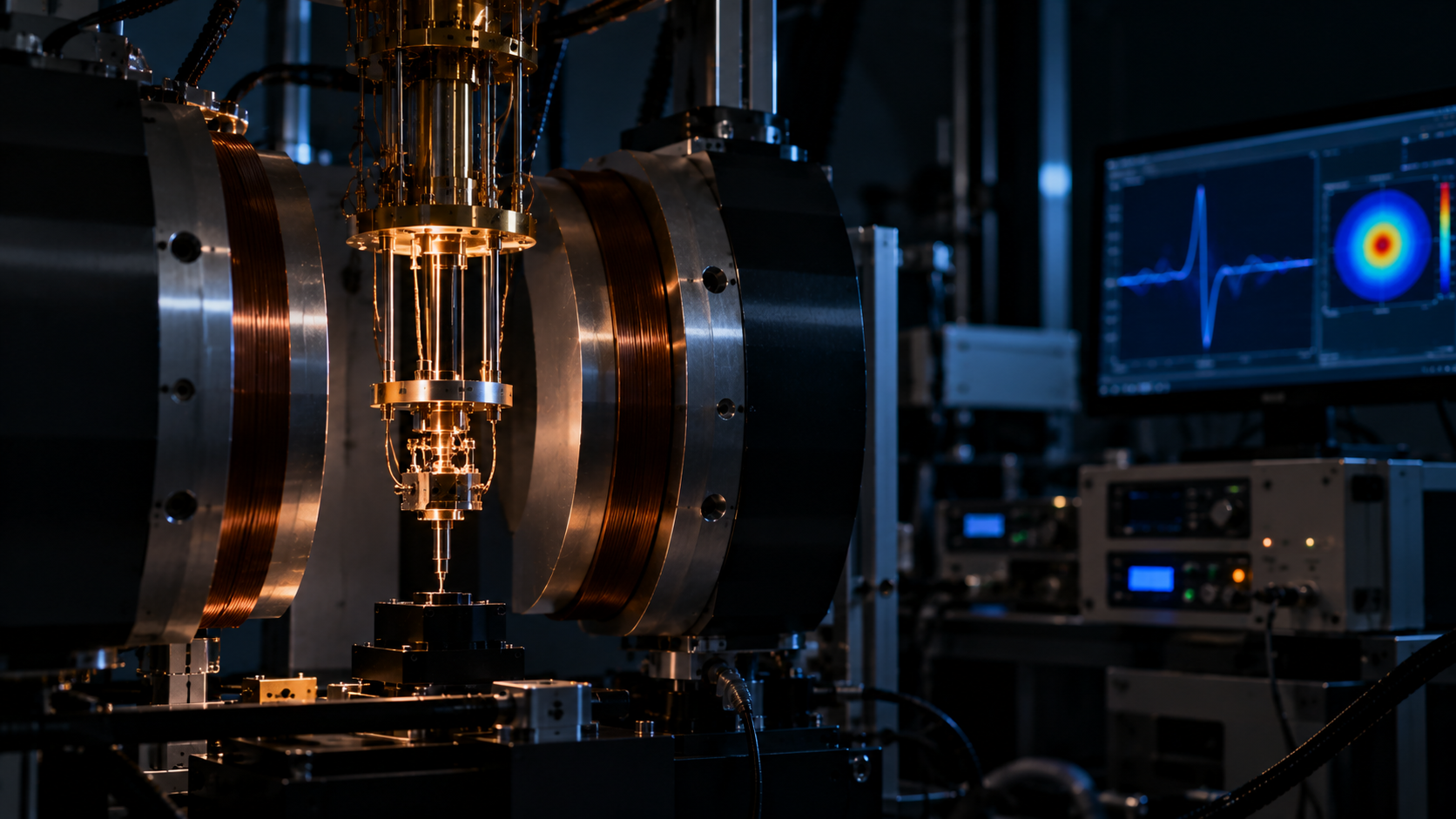
EPR / Magnetic Resonance
Investigate paramagnetic species, free radicals and spin behavior.
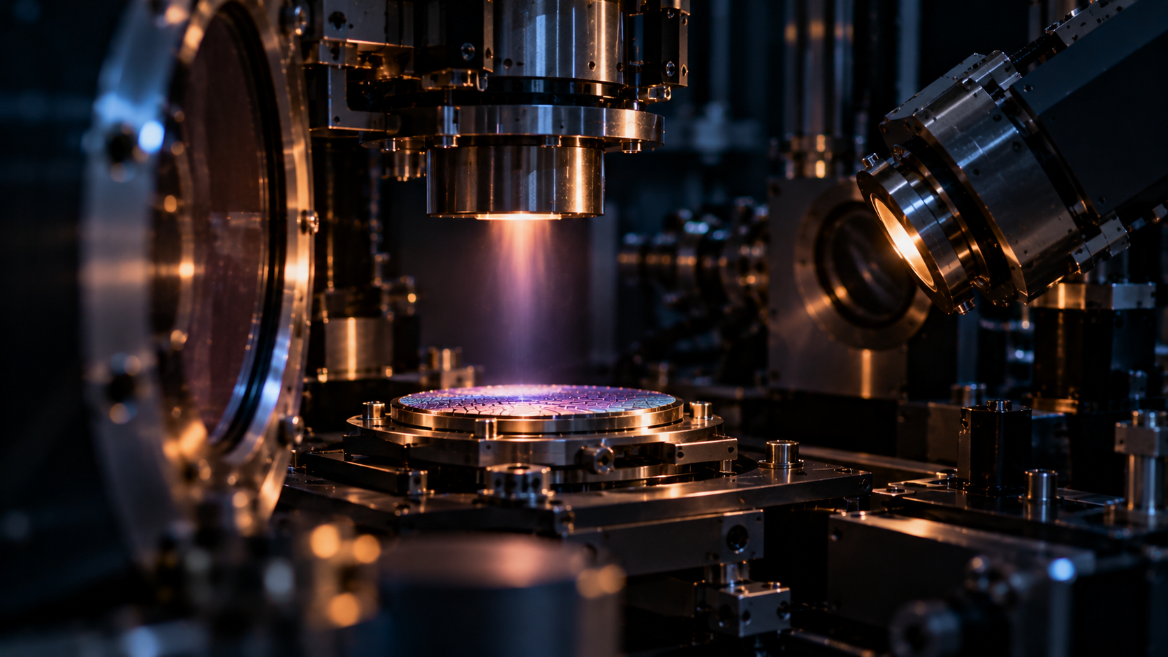
Nanotechnology
Develop and study nanostructures, coatings and functional materials.
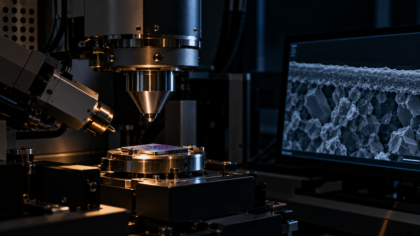
Materials Characterization
Connect composition and structure to material performance.
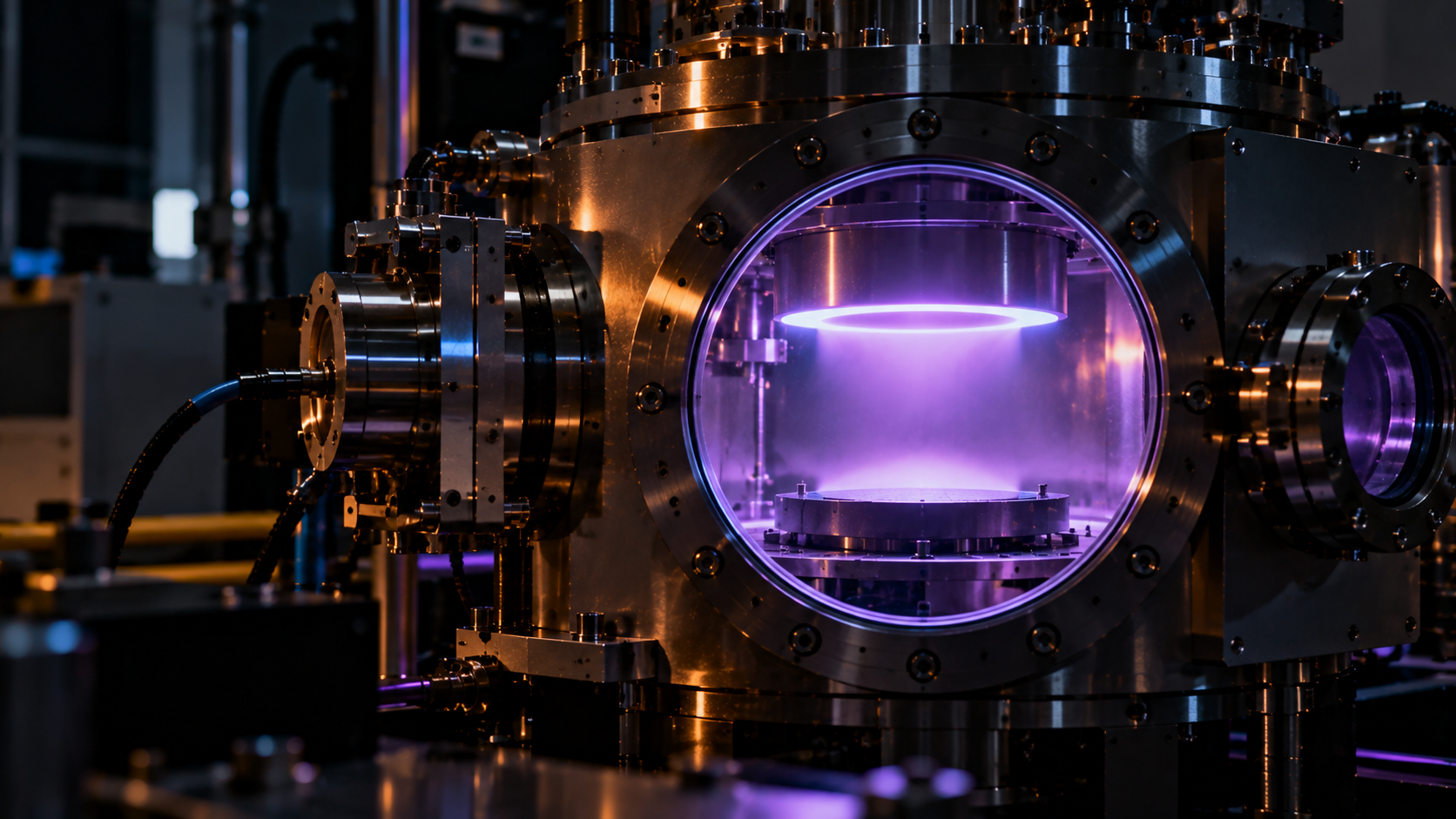
Plasma Processing
Use controlled plasma environments for deposition and surface engineering.
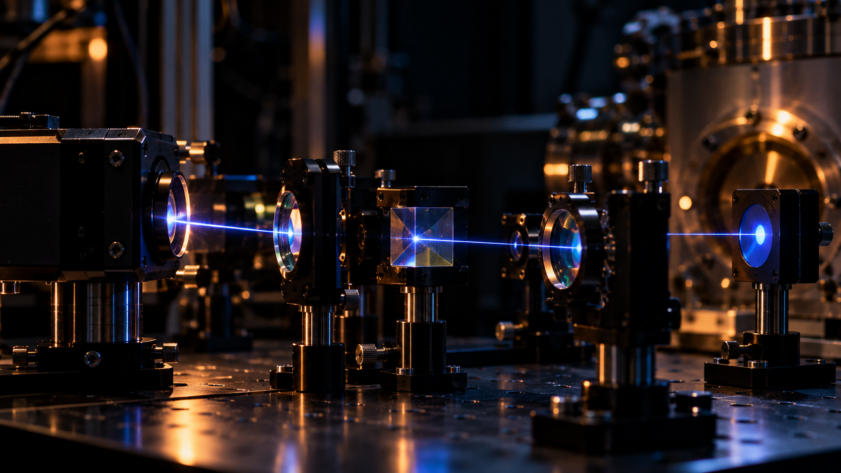
Photonics
Enable optical measurement, light–matter research and precision experiments.
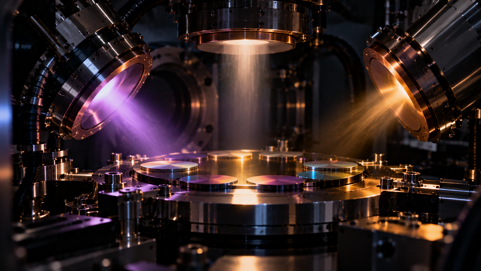
Surface Engineering & Coatings
Develop wear-resistant, functional and decorative coatings for demanding surfaces.
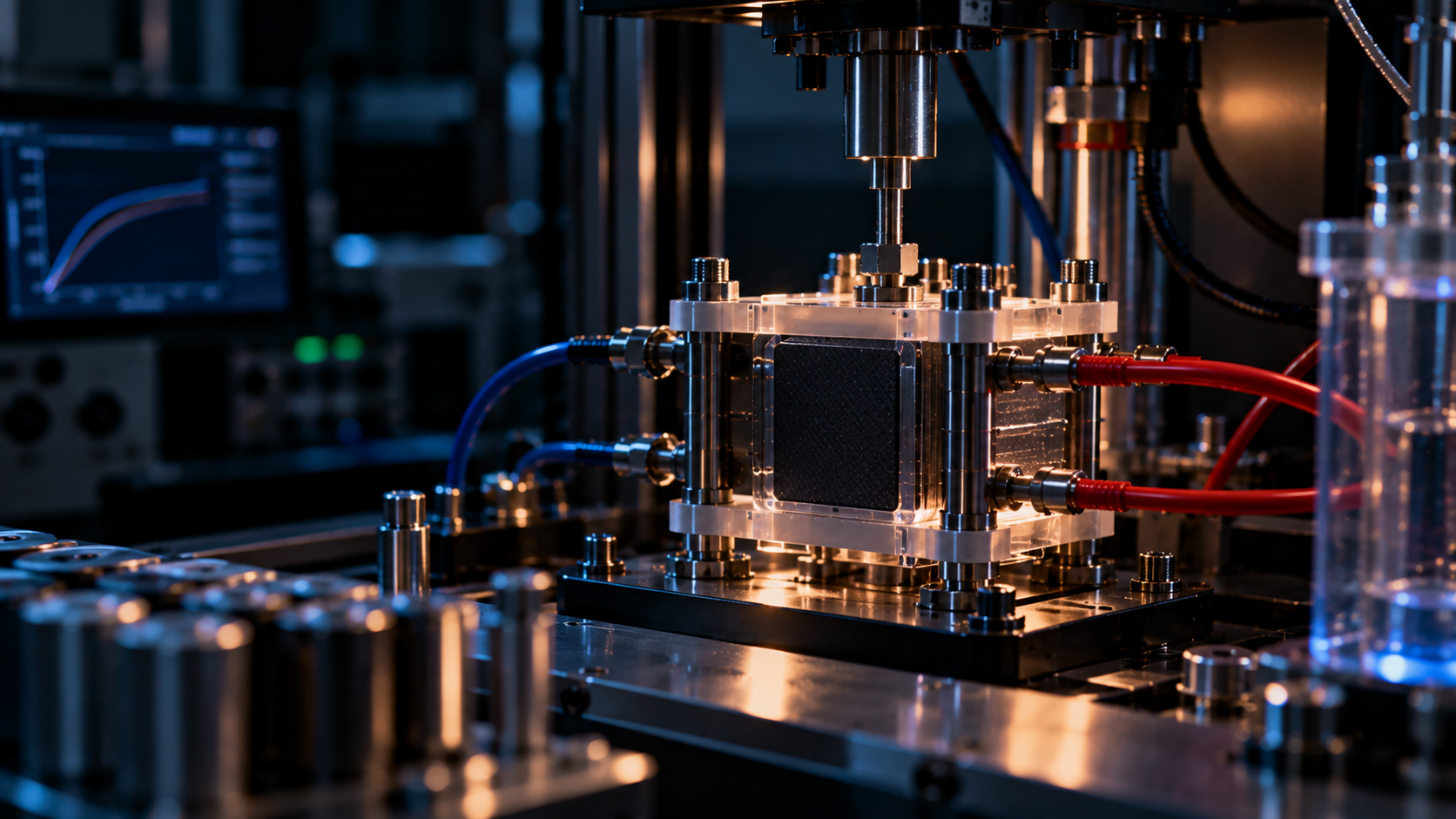
Energy & Electrochemical Materials
Advance fuel cell, battery and electrochemical materials research.
Tell us what you are working on.
Start with the research objective. We’ll help connect the requirement to the right technology path.
Discuss your requirement